Electromagnetic metamaterials
We develop electromagnetic metamaterials across optical, terahertz, and microwave/RF regimes, enabling finely controlled light–matter interactions and advanced wave manipulation. Using powerful modelling tools and specialised optical and microwave facilities, we translate fundamental discoveries into applications in communications, imaging, energy, aerospace, healthcare, and defence.
In this section

Our research
Controlling the interaction between light and matter is fundamental to science and technology – from probing entanglement in quantum physics to harnessing the spectacular information carrying capacity of optical fibres. Nanoscale fabrication techniques, such as electron-beam lithography, allow us to create new materials with increasing sophistication and freedom of design, however controlling light at the nanoscale remains a challenge.
Our research
Our work in optical metamaterials spans from investigations of fundamental light-matter interactions to applications-driven research for sectors such as green energy generation and medical imaging.
We investigate a variety of topics such as:
- the tunable optical responses of active / reconfigurable optical metasurfaces (ordered and disordered),
- the development of new imaging techniques using the precise shaping of light ('structured light') to control how light propagates inside opaque scattering materials,
- the control of light below the wavelength limit using localised resonances on metallic nanostructures ('plasmonics'),
- the generation of new photonic modes by overlapping the optical response of two materials ('strong coupling'),
- bio-photonic inspired nanostructures.
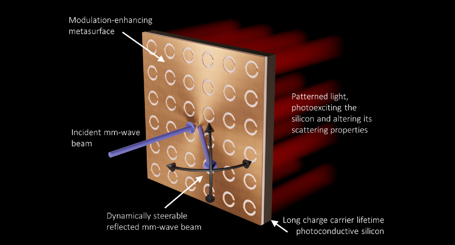
To date, most of the research into surface plasmon resonances has been limited to frequencies near metallic plasma frequencies (i.e. in the visible spectral region). Semiconductors, such as graphene, with plasma frequencies in the THz and IR spectral ranges, offer the potential for confining surface plasmon resonances at lower frequencies. Furthermore, semiconductors offer a unique and hugely beneficial advantage over metals: since the surface charge density can be modified by, for example chemical doping, plasma frequencies and SPP properties can be tailored. An extension of this is the exciting possibility of all-optical plasmon control, i.e. ‘photo-doping’ a semiconductor with visible frequency light, so that plasma frequencies may be tuned by a visible frequency light source, allowing active materials that can be switched on very fast (picosecond) timescales, something that is essential for high-bandwidth and/or time resolved applications.
Our research focusses on developing and studying structured materials (metamaterials) that exhibit novel and valuable electromagnetic behaviours. These behaviours arise uniquely from their structure, and through controlling their geometry at a subwavelength scale, we can produce metamaterials with properties far beyond those found in traditional materials. Our research is focusses both on addressing the fundamental research challenges associated with designing, fabricating and testing these materials, to working with industrial partners to utilise metamaterials to tackle real world problems.
Our research
Some of the areas we work in are:
- Novel materials and design approaches for antennas.
- Control over surface impedance for manipulating reflection from flat and curved surfaces.
- Surface wave transport.
- Superscattering and retroreflective materials.
- Shape-morphing and for reconfigurable, or environmentally responsive electromagnetic materials.
Real-world applications
The importance of the microwave and RF region of the electromagnetic spectrum for applications ranging from telecommunications to wireless power transfer has nurtured a huge demand for materials to build smaller, lighter, more versatile components. Metamaterials have the potential to achieve these goals, and we use our expertise, alongside that of partners across academia, industry and government agencies, to apply our research to real world problems ranging across sectors as diverse as:
- Aerospace
- Healthcare
- Defence and security
- Telecommunications
Facilities
- Capability from 70kHz – 110 GHz using multiple Vector Network Analysers (VNAs).
- Horn antennas that can be utilised from 800-1000 MHz and 5 to 110 GHz.
- Microwave benches with rotating stages that provide a collimated (distance source) beam to determine the response of test samples as a function of angle of incidence.
- A fully-lined anechoic chamber for antenna and/or scattering measurements.
- A computer controlled xyz-scanning stage and near-field probes provides the ability to measure the intensity and phase of the electromagnetic fields scattered from objects under test, and across surfaces.
- We also have a 65 GSa/s Arbitrary Waveform Generator coupled to a 4 channel oscilloscope with 25 GHz of real-time bandwidth.
For optical measurements, we have a vast array of laser systems from manufacturers such as Coherent, Carl Zeiss, Thorlabs and Spectra-Physics. Our range of continuous (CW) and pulsed lasers grant us access to a huge parameter space (controlling average power, peak power, wavelength and pulse duration) that enable us to perform novel experiments.
- Cleanrooms
- We have two in-house state of the art cleanrooms covering a total area of 150 m², providing ISO Class 5 and ISO Class 6 environments for micro- and nanofabrication. The following tools support the fabrication of micro and nano photonic structures, visible to infrared metamaterials, microfluidic components, optoelectronic devices, micromechanical systems, sensors and biomedical microstructures.
- Lithography
- High resolution patterning capability through: A NanoBeam NB4 100kV electron-beam lithography system, capable of producing features down to ~10 nm on a variety of substrates up to 150 mm; Microlight3D microFAB-3D.Advanced two-photon polymerisation (2PP) lithography tool for direct-write 3D microfabrication, producing free-form polymer structures with feature sizes down to ~200 nm; Durham Magneto Optics Microwriter ML direct-write laser system (405 nm), a Karl Suss MJB4 i-line mask aligner and a Kloe UV-Kub 2 UV exposure system.
- Thin-film deposition
- High quality thin film material deposition (metallic and dielectric) through: HHV TF500 sputterer and Auto306 thermal evaporator; Lesker PVD75 combined electron-beam and thermal evaporator; Moorfield nanoPVD S10A benchtop sputtering system.
- Dry etching
- Plasma etching and surface processing capability through: JLS Designs RIE80 RF / ICP Reactive Ion Etching system, and Moorfield NanoETCH.
Supporting fabrication equipment includes a dicing saw (LoadPoint Micro Ace 3 Dicing Saw), wire bonders (K&S 4123 and 4700 Wire Bonders) and a critical-point dryer. Metrology includes optical microscopy (Nikon LV150 Upright Microscopes), scanning electron microscopy, surface profilometry (KLA-Tencor D-100 Surface Profiler) and an electrical 4-point probe station.
We have complementary metrology and characterisation tooling, including an Imaging Suite, which includes focused ion beam and electron microscopy (TESCAN VEGA3 SEM, xT Nova Nanolab 600 FIB SEM, JEOL 2100 TEM), x-ray diffraction (Bruker D8 advanced XRD), atomic force microscopy (Bruker Innova AFM), FTIR microscope (Bruker LUMOS II) and automated 3D light microscope (Keyence VHX-7000).
Our centre has access to facilities that include
- Additive Manufacturing
- Large Format, high temperature printing
- laser sintering systems (including metal printing)
- material extrusion
- Materials processing and manufacturing
- including injection / compression moulding and extrsuion
- Materials analysis, including
- thermal (Differential Scanning Calorimetry, Thermogravimetric analysis, Dynamic Mechanical Analyis)
- spectroscopy (FTIR, NIR. UV)
- microscopy
- rheology
- surface analysis
- Mechanical Testing, including drop towers and impact testers
- Vacuum Forming
- CAD/CAM software
Many of these facilities can be accessed via Exeter technologies Group.
- We are advanced users of Ansoft HFSS, CST Microwave studio and Comsol Multiphysics for numerical modelling of electromagnetic and acoustic systems. Differential methods for predicting the response of multilayered corrugated surfaces (diffraction gratings) have been developed, together with modal matching analytical techniques for predicting the response of well-defined photonic structures.
- We can predict the properties of magnetic nano-structures and devices using the MuMax simulation software, and permits the study of dynamical phenomena, such as spin waves in magnetic nanostructures (magnonics) and the kinetics of magnons.
- Our team have expertise in the development of finite difference time domain (FDTD) methods for predicting the MHz and GHz response of metamaterials, including the incorporation of the Landau-Lifshitz-Gilbert equation for the study of magnetic materials. This work is a University spin-out company, www.MaxLLG.com.
People
Our researchers in this area include:


Dr Cameron Gallagher
Senior Industrial Research Fellow (Metamaterials)
C.Gallagher2@exeter.ac.uk Exeter


Metamaterials driving solar panel innovation
Find out more